


CONTRIBUTE TO CUSTOMERS’ VALUE CREATION WITH INNOVATIVE IDEAS About Nitto
Nitto leverages in-house developed technologies to gain competitive advantages for its customers. We do so by staying close to our customers, understanding their challenges, and co-creating materials and services that answer the needs of all stakeholder, including society and the environment. Nitto offers advanced process materials for the semiconductor industry. We are creating the next wonders for the world. Now and forever. Innovation for Customers.
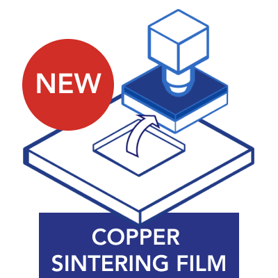
UNIFORM & STABLE BTL/BONDING SURFACE COPPER SINTERING FILM

Nitto is pioneering in rising demands for efficient and cost-effective heat management solutions. Our innovative copper sinter film offers easy handling after die attach (pre-bonding) and ensures a stable bonding line thickness, all while leveraging the cost benefits of copper over silver. It supports direct sintering on copper, gold, and silver, and its offers excellent opportunities for clip-to-die and module-to-heatsink applications. Additionally, it is free from hazardous or harmful organics and binders.
HIGH THERMAL CONDUCTIVITY
STABLE BONDING LINE THICKNESS
GOOD HANDLING AND PRE-BONDING
UNIFORM BONDING SURFACE AFTER SINTERING
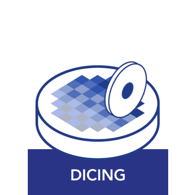
PRESENT IN EVERY STEP OF THE SEMICONDUCTOR PROCESS

The Cleaning Wafer™ is a highly efficient particle remover featuring a cleaning layer allowing for a constant semiconductor production workflow. Down-time of tools can be drastically reduced compared to conventional hand cleaning. The Cleaning Wafer™ can also be used for maintenance to improve long-term performance. Nitto's solution for clean wafers is applicable in vacuum chambers in semiconductor front-end and mid-end process of semiconductor manufacturing equipment. Go to product page.
HIGHLY EFFICIENT PARTICLE REMOVER
ENABLING CONTINUOUS WORKFLOWS
REDUCING DOWNTIME

Nitto has a line-up of various equipment that perform tape processing on semiconductor wafers, which can fully support the main needs during devices production. By maximizing the tape's original functions, Nitto supports the production of thinner wafers and new devices technology with the maximum expertise, by supporting the partners with all-in one solution. Go to product page.
EASY PEELING WITHOUT RESIDUE
LOW TOTAL THICKNESS VARIATION
HEAT & CHEMicAL RESISTANT TYPES

With extensive experience and a comprehensive line-up of pressure-sensitive and UV-curable dicing tapes, Nitto is well-equipped to support processes. Additionally, we stay at the forefront of new dicing technologies, including stealth, laser full-cut, and plasma dicing. Our focus also extends to incorporating advanced functionalities such as solvent resistance, anti-whisker properties, and laser mark visibility for package dicing. Our tapes’ outstanding characteristics enhance the efficiency and reliability of the wafer manufacturing dicing process.Go to product page
NO ADHESIVE RESIDUE
ANTI- WHISKER
CHEMICAL RESISTANCE AVAILABLE
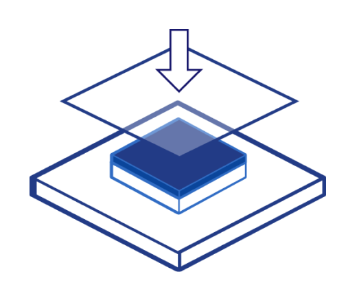
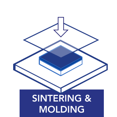
NITOFLON™, a high-performance fluoroplastic (PTFE) film, is the ideal choice for supporting thermal compression bonding and molding/sintering processes in semiconductor applications. Tailored to meet specific requirements, NITOFLON™ enhances production efficiency and ensures superior performance..Go to product page
GOOD RELEASABILITY
DEFORMATION CONTROL
CUSHIONING EFFECT
HEAT RESTISTANCE